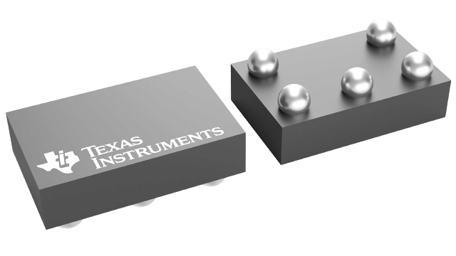

SN74LVC1G125YZPR
Single 1.65-V to 5.5-V buffer with 3-state outputs
Factory Direct Sales, Lower Price for Bulk Purchase
Min. Order: 3000
Packaging information
Package | Pins
DSBGA (YZP) | 5
Operating temperature range (°C)
-40 to 125
Package qty | Carrier
3,000/Reel

Description
Reviews
Features for the SN74LVC1G125
- Available in the Ultra Small 0.64-mm2
Package (DPW) With 0.5-mm Pitch - Supports 5-V VCC Operation
- Inputs Accept Voltages to 5.5 V
- Provides Down Translation to VCC
- Max tpd of 3.7 ns at 3.3 V
- Low Power Consumption, 10-μA Max ICC
- ±24-mA Output Drive at 3.3 V
- Ioff Supports Live Insertion, Partial-Power-Down Mode, and Back-Drive Protection
- Latch-Up Performance Exceeds 100 mA
Per JESD 78, Class II - ESD Protection Exceeds JESD 22
- 2000-V Human-Body Model (A114-A)
- 200-V Machine Model (A115-A)
- 1000-V Charged-Device Model (C101)
Description for the SN74LVC1G125
This bus buffer gate is designed for 1.65-V to 5.5-V VCC operation.
The SN74LVC1G125 device is a single line driver with a 3-state output. The output is disabled when the output-enable (OE) input is high.
The CMOS device has high output drive while maintaining low static power dissipation over a broad VCC operating range.
The SN74LVC1G125 device is available in a variety of packages including the ultra-small DPW package with a body size of 0.8 mm × 0.8 mm.
Share your thoughts
Showing
6
of
0
reviews
Most recent
Top Reviews
Read more
Your rating
Your review *
Name *
Enter your Name
Email *
Enter your Email
Upload Image
Notice: Ensure your image is no larger than 200KB before uploading.
Submit
Contact Us Now
Enter your inquiry details, We will reply you in 24 hours.
Name can't be empty
E-mail can't be empty
Company can't be empty
Phone can't be empty
Phone
Products can't be empty
Products you want
Message can't be empty
Verification code error
Clear
People who viewed this item also viewed

