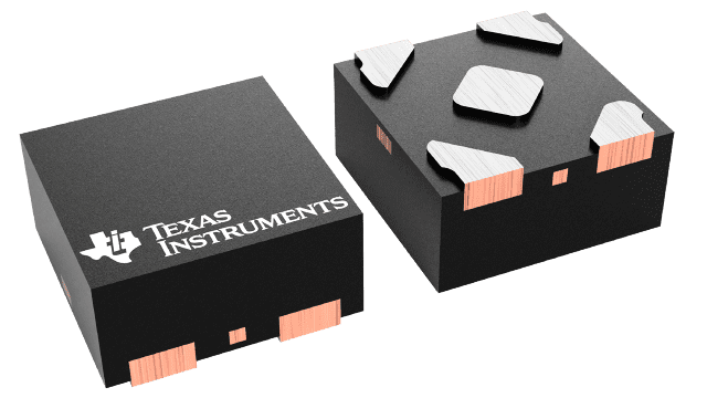

CDCBT1001DPWR
1.2-V to 1.8-V clock buffer and level translator
Factory Direct Sales, Lower Price for Bulk Purchase
Min. Order: 3000
Packaging information
Package | Pins
X2SON (DPW) | 5
Operating temperature range (°C)
-40 to 85
Package qty | Carrier
3,000/Reel

Description
Reviews
Features for the CDCBT1001
- Clock frequency range: DC to 24 MHz
- 1.2-V to 1.8-V LVCMOS clock level translation:
- VDD_IN = 1.2 V ± 10%
- VDD_OUT = 1.8 V ± 10%
- Low additive jitter and phase noise:
- 0.8-ps maximum 12-kHz to 5-MHz additive RMS jitter (fout = 24 MHz)
- –120-dBc/Hz maximum phase noise at 1-kHz offset (fout = 24 MHz)
- –148-dBc/Hz maximum phase noise floor (fout = 24 MHz, foffset ≥ 1 MHz)
- 5-ns 20% to 80% rise/fall time
- 10-ns propagation delay
- Low current consumption
- –40°C to 85°C operating temperature range
Description for the CDCBT1001
The CDCBT1001 is a 1.2-V to 1.8-V clock buffer and level translator. The VDD_IN pin supply voltage defines the input LVCMOS clock level. The VDD_OUT pin supply voltage defines the output LVCMOS clock level. VDD_IN = 1.2 V ± 10%. VDD_OUT = 1.8 V ± 10%
The 12-kHz to 5-MHz additive RMS jitter at 24 MHz is less than 0.8 ps.
Share your thoughts
Showing
6
of
0
reviews
Most recent
Top Reviews
Read more
Your rating
Your review *
Name *
Enter your Name
Email *
Enter your Email
Upload Image
Notice: Ensure your image is no larger than 200KB before uploading.
Submit
Contact Us Now
Enter your inquiry details, We will reply you in 24 hours.
Name can't be empty
E-mail can't be empty
Company can't be empty
Phone can't be empty
Phone
Products can't be empty
Products you want
Message can't be empty
Verification code error
Clear
People who viewed this item also viewed

